Hard Tech Enablers: The Solutions Reshaping Semiconductor Technology
As we explored in Part 1 of our two part series, the semiconductor industry faces unprecedented challenges in meeting AI's computational demands. However, a wave of innovations is emerging to address these challenges. From novel manufacturing approaches to revolutionary thermal management solutions, let's explore how the industry is adapting to power the next generation of AI computing.
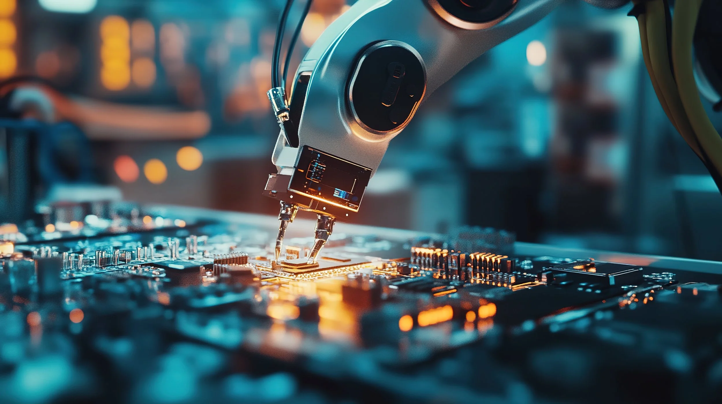
Next-Generation Manufacturing Solutions
The industry's approach to manufacturing more powerful chips is evolving rapidly. Traditional lithography processes, while still crucial, are being augmented by innovative new approaches. For instance, companies are developing "dry resist" technologies that can help improve the precision of this critical step. While these solutions currently cost about three times more than traditional methods, their potential for higher yields and better performance makes them increasingly attractive as chip complexity grows.
Another critical advancement lies in Chemical Mechanical Planarization (CMP), which creates the ultra-flat surfaces essential between manufacturing steps. As chip designs now feature up to 15 layers of metallization and incorporate new hybrid bonding approaches, CMP is instrumental in achieving the precise alignment these complex architectures demand, and continued innovation is required to deliver ever smaller nodes while keeping yields high. .
The 3D Revolution: Building Upward, Not Outward
When traditional two-dimensional scaling becomes prohibitively expensive or technically challenging, the industry is increasingly looking upward. Advanced packaging technologies, particularly 2.5D and 3D approaches, are transforming how we build high-performance chips.
Some companies are pioneering new approaches using glass and low-stress polymers instead of traditional silicon interposers. This technology, while still early in its development, demonstrates impressive metrics at the lab scale:
50% improvement in bandwidth and signal performance
50% reduction in power consumption
Ability to handle substrates up to 10x larger than traditional approaches
This shift to advanced packaging isn't just about performance – it's about practical scalability. As one industry expert noted during our recent discussion, "We're seeing companies achieve things with 3D packaging that would be impossible with traditional approaches, particularly in AI applications."
Thermal Innovation: The Cool Factor
Perhaps some of the most exciting innovations are happening in thermal management. Two distinct approaches are showing particular promise:
Carbon Nanotube Solutions
Aligned carbon nanotube arrays can dramatically improve heat dissipation. This technology has demonstrated superior long-term performance compared to traditional thermal interface materials, maintaining consistent performance even after thousands of thermal cycles.
Copper Nanostructure Approaches
Novel copper-based solutions, use roll-to-roll printed copper nanostructures backfilled with eutectic metals. This approach offers two product tiers:
A cost-competitive option for standard applications
A premium solution offering significantly better thermal resistance for high-performance computing
The Evolution of Photonics: Next-Generation Computing
While much attention focuses on traditional semiconductor approaches, photonics represents a potential paradigm shift in computing architecture. Silicon photonics is evolving from a technology primarily used in long-distance communication to one that could revolutionize chip-to-chip communication. The landscape of companies driving this evolution reveals diverse technological approaches. Established players like Intel and Cisco continue advancing traditional silicon photonics, but newer entrants are exploring more radical innovations. Pangaea's investment in Aeponyx exemplifies this evolution. Aeponyx’s silicon nitride platform offers superior optical performance over traditional silicon, bridging the gap between conventional approaches and next-generation materials.
Recent innovations in electrical-optical conversion materials show particular promise. While traditional technologies hit performance limits around 100 gigabits per second, new approaches using materials such as lithium niobate, barium titanate and liquid crystal polymers are pushing these boundaries further. Lithium niobate, first explored at Bell Labs over 50 years ago is finally approaching commercial viability. Meanwhile, ferroelectric pneumatic liquid crystals have demonstrated superior performance without the durability issues that plague other organic materials.
Capturing the imagination of investors are companies like Light Matter and Celestial AI, which have attracted valuations exceeding $1 billion for their work on photonic fabric solutions. These companies are developing co-packaged optics that bring photonic capabilities directly to the computational core - though they remain pre-commercial, their approaches represent significant bets on the future of photonics . Some earlier stage companies are pushing the boundaries even further, using materials approaches to solve massive size challenges in photonic computing. For example, photononic components such as waveguides and resonators necessarily require substantially larger footprints than their electronic counterparts. However, recent innovations suggest photonic solutions could potentially achieve massive reductions in size footprints while also increasing energy efficiency.
Investment Considerations: What Makes a Winner?
For investors and founders in this space, several key factors differentiate successful ventures:
Mission-Critical Solutions: Successful companies address fundamental industry challenges rather than incremental improvements.
Clear Value Capture: The ability to demonstrate quantifiable impact on cost-per-wafer or chip performance.
Defensive IP Position: Unique intellectual property that provides lasting competitive advantages.
Strong Partnerships: Relationships with major industry players that validate the technology and provide paths to market.
Capital Efficiency: Smart deployment of resources given the capital-intensive nature of semiconductor development.
Industry Experience: While the perseverance and creativity of a new founder can be priceless in this market, significant industry experience is also a must.
Looking Ahead
The semiconductor industry's ability to innovate has never been more critical. As AI continues to drive demand for more powerful computing solutions, these technological advances will play a crucial role in enabling the next generation of applications.
Success in this space requires more than just technical excellence – it demands a deep understanding of industry dynamics, strong partnerships, and the ability to execute in a highly complex ecosystem. Companies that can deliver solutions addressing multiple challenges while maintaining manufacturability and cost-effectiveness will be particularly well-positioned.
The next few years will likely see continued acceleration in innovation as these technologies mature and new approaches emerge. For investors, founders, and industry observers, understanding these trends and their implications will be crucial for navigating the evolving semiconductor landscape.